Since the isolation of graphene, we have identified a number of materials that form atomically thin sheets. Like graphene, some of these sheets are made from a single element; others are formed by chemicals where the atomic bonds naturally create a leaf-like structure. Many of these materials have different properties. While graphene is an excellent conductor of electricity, a number of other semiconductors are. And it’s possible to further fine-tune their properties based on how you arrange the layers of a multi-sheet stack.
Given all those options, it shouldn’t surprise anyone that researchers have figured out how to make electronics from these materials, including flash memory and the smallest transistors ever made. However, most of these are demonstrations of the ability to create the hardware – they are not integrated into a usable device. But a team of researchers has now shown that it’s possible to go beyond simple demonstrations by building a 900-pixel image sensor using an atomically thin material.
Making pictures
Most image sensors currently consist of standard silicon semiconductors fabricated using the usual complementary metal-oxide semiconductor (CMOS) processes. But it is possible to replace the silicon with another semiconductor. In this case, the researchers used molybdenum disulfide, an atomically thin material that has been widely used in experimental devices.
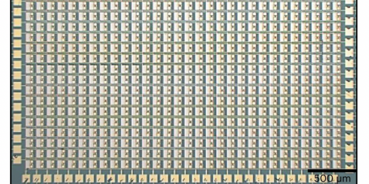
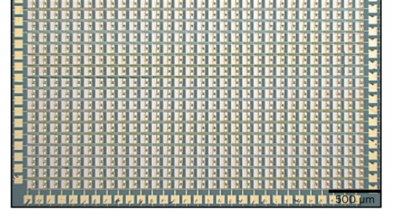
To use this in a device, the researchers started by growing a single-layer sheet of molybdenum disulfide on a sapphire substrate using vapor deposition. It was then lifted off the sapphire and lowered onto a previously created silicon dioxide surface that already had some wiring etched in it. Further wiring was then deposited on top.
The end result of this process was a grid of 30 by 30 devices, where each device consists of a source and drain electrode connected by a sheet of molybdenum disulfide. When illuminated, each of these devices would pick up stray charges, affecting their ability to transfer current between the source and drain electrodes. That difference in resistance provides a measure of how much light the device is exposed to, allowing image information to be reconstructed.
While the charges that accumulate after exposure to light slowly dissipate on their own, most devices actively clear them by applying a strong voltage between the source and drain electrodes.
Good and bad
If you compare this to a standard silicon sensor, it’s a bit of a mixed story: better in some ways, notably worse in others. On the good side, the devices require remarkably little power to operate; the researchers estimate that less than a picoJoule is needed per pixel during operations. Resetting the device remains a simple process of applying a large voltage difference across the molybdenum disulfide sheet.
The researchers found that applying a much smaller voltage across the molybdenum disulfide sensitizes it to light. This allows easy adjustment of the signal-to-noise sensitivity of the image sensors during use. Typically, this requires a fair amount of external circuitry on silicon-based imaging hardware, with a corresponding increase in fabrication complexity and power consumption during imaging. This device therefore offers a number of advantages.
What it doesn’t offer is speed. While the initial response to light can be registered in just 100 nanoseconds, a full high-contrast exposure takes seconds – per color. So a blue exposure takes more than two seconds and the red channel takes almost 10 seconds for a full exposure. So don’t expect to use this to shoot some quick videos on your mobile phone.
Of course, this doesn’t mean it’s useless; it just limits what it’s useful for. There are plenty of applications where power is more of a constraint than time, such as environmental sensors and the like (the people who developed it are excited about IoT applications). But the bigger story here may be that the researchers built a rather large, complicated device that relies on atomically thin material.
Natural materials2022. DOI: 10.1038/s41563-022-01398-9 (About DOIs).